American Semiconductor Demonstrates SoP-HEMI™ Spherical CHIPS for Ocular and Image Sensor Applications

A flexible die mounted on a spherical surface

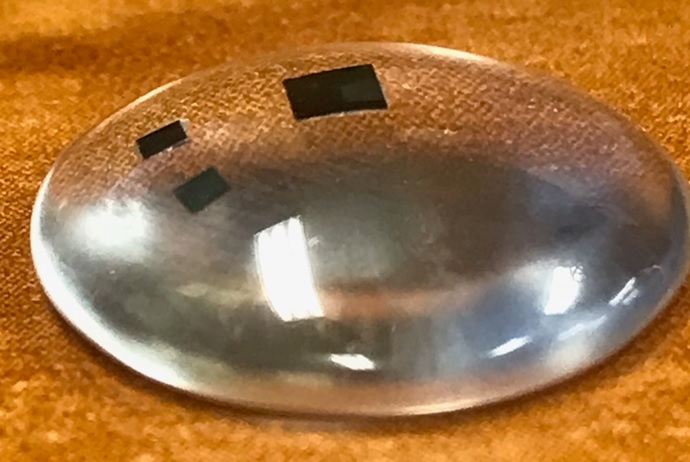
In another display of American innovation, American Semiconductor (ASI) demonstrated spherical IC assembly resulting from continued research and development of the U.S. company’s Semiconductor-on-Polymer WLCSP process. ASI is well known for making the thinnest ICs in the world by applying its Semiconductor-on-Polymer WLCSP process to a variety of chips. Applications to date have focused on utilizing the radically thin advanced packaging technology’s ability to bend or twist. The new work demonstrates dome shaped or “Hemi” ICs that enable advances in smart-contacts, ocular implants and image sensors.

If you are interested in collaborating in regards to this innovative technology, let us know via our Contact Page or our email at sales@americansemi.com

 SoP-TM™, the industry’s first wafer level CSP fully protected process has been released for customer use. The unique process features polyimide encasement on all 6 sides of the die. New product developments utilizing ultra-thin and/or flexible electronics have suffered for lack of the test chips needed to develop next generation advanced manufacturing processes. Thin, bare silicon is not sufficient for this requirement. 

Full function ICs are difficult to easily test and can be expensive to use for process development. Many new applications need chip scale packaged (CSP) ICs with full chip encapsulation for protection against damage and environmental exposure. American Semiconductor has released a new line-up of SoP-TM™ (6 side protected) CSP Test Chips that are designed for use in adoption of the new packaging technology.

These ultra-thin test chips include a variety of on-chip interconnects that enable quick and efficient testing of new assembly process capability. See the new Test Chips here.

For more information contact us at here.

Share This